The production of electrical circuits is a delicate task that requires precision and quality from…
What is SMD assembly with AOI?
SMD assembly with AOI has been growing in importance in recent months. It is an essential combination to ensure the reliability of electronic products in different sectors, such as the automotive or medical sectors. To make known what this technique consists of, Electrolomas has created this content that explains it in a clear and simple way.
Nature and features of SMD assembly
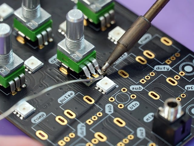
Surface Mount Device (SMD) technology is a widely used process in the manufacture of electronic circuits. It is characterized by the placement of components directly on the surface of a Printed Circuit Board (PCB). Unlike conventional techniques, this does not require perforations, which allows for more compact and lightweight designs.
As for the assembly process itself, it begins with the application of a solder paste on the contact points of the PCB. Automated placement machines then place the components on the paste, which is then melted in an oven to ensure the correct electrical connection of the different elements.
The main characteristics of SMD assembly include reduced device size, increased component density and greater efficiency in large-scale production. This type of assembly also favours the development of more complex and multifunctional devices, such as mobile phones, laptops and telecommunications equipment.
Its versatility and precision make it a fundamental option for the manufacture of high-tech electronic products, where space optimisation and performance are crucial. This is precisely what today’s industry demands in order to offer devices that provide value to the end user.
What is an AOI system?
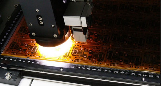
The Automated Optical Inspection (AOI) system is a technology designed to detect defects and ensure the quality of printed circuit assemblies. Using high-resolution cameras and image processing algorithms, electronic components and solder joints are examined for irregularities, allowing problems to be identified before the final product is assembled or shipped to the customer.
The AOI system begins by capturing photographs of the circuit board as it moves through a production line. These images are compared to a reference model to discover errors, whether they are incorrectly placed components, defective solder joints or short circuits.
In addition to the above, this system makes a difference due to its speed in detecting errors, its ability to carry out exhaustive inspections without human intervention and its high precision. This technology not only increases the efficiency of the manufacturing process, but also contributes to the reduction of costs by minimising the risk of failure in final products.
Thanks to an SMD assembly with an AOI system, a better final product is achieved. Efficiency is gained, the risk of failure is reduced and production processes are simplified. In this way, it is possible to develop better devices that meet the needs of customers. At Electrolomas we provide quality services based on cutting-edge technologies. Contact us now!
Related Posts